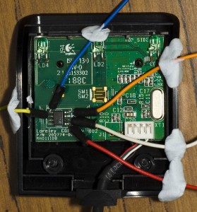
So I’m playing around more with the Scanalogic 2 Pro and thought instead of just reading the Logitech LX310 receiver’s EEPROM I would actually probe it and see what’s going on when it starts up. My plan for this post is to make it as simple and easy to follow as possible.
As you might know it’s a ST 95160 16Kbit EEPROM which is uses SPI protocol; I’ve found that SPI is harder to understand and use than two-wire (I2C) protocol. I used the Arduino SPIEEPROM page to assist me as well as the datasheet which once you read parts of it enough times and see what’s happening in the logic actually starts to make sense 😛
Download the complete timeline of SPI communication here: Logitech LX310 Reciever SPI 10Mhz
You’ll need to download the Scanalogic software in order to use the above file. Please note that the ms timeline shown in these pictures may be different to the timeline you download, however all queries are still the same.
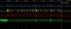
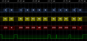
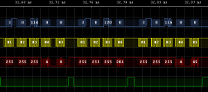
Here is an overview of the first 10ms upon connecting to my computer.
What I suspect we see up to the first millisecond is the chip in the receiver is initialising itself by looking at the CS line as it’s going high and low very quickly, plus it could just be the rush of power to it causing the CS to go all funny.
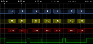
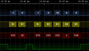
What these channels in the picture do:
MOSI (blue) – The input line to the EEPROM, used to send commands like read, write, etc.
CLK (yellow) – The clock to the EEPROM, used to divide our requests.
MISO (red) – The output line from the EEPROM, used to receive data and results to queries.
CS (green) – Select the EEPROM for use, allows you to use other devices that are on the SPI bus.
Commands we can send to the EEPROM:
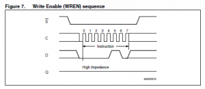
Write Enable: 6 – Enable the EEPROM for writing.
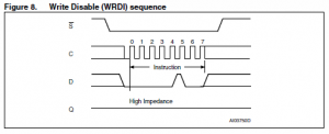
Write Disable: 4 – Disable the EEPROM for writing.
Read Status Register: 5 – Read the place certain parameters of the EEPROM is set
Write Status Register: 1 – Write to the place certain parameters of the EEPROM are set
Read: 3 – Read data from the EEPROM
Write: 2 – Write data to the EEPROM
Take note of the channels and commands with numbers as above, we’ll be referencing the commands/number for all of this guide.
As you can see it’s all very structured.
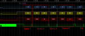
A quick way to see each query is to look at the CS (green) line. Once it drops to low and then goes back to high again, this indicates the first query. The CLK (yellow) can also identify this by showing how spaced apart each 8 highs/lows are. The MOSI (blue) is the data we are feeding into the EEPROM and the MISO (red) is the data coming out from the EEPROM. Sometimes no “real” result is expected from the data we feed into the EEPROM.
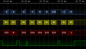
Now lets jump in and analyse after the first millisecond query by query.
Query 1
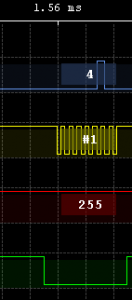
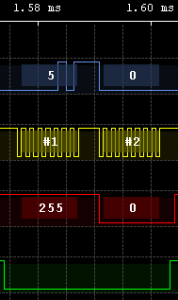
First query we send is 4 which is a Write Disable, it actually sets a variable called the “Write Enable Latch” to 0 which blocks us from writing to the EEPROM, think of it as cheap insurance; as we are booting up our micro-controller could have already started sending all kinds of weird data. Now if you look at the output it’s 255, think of this as a way the EEPROM is saying that it’s listening to us.
As per the data sheet page 17, we shouldn’t expect a result back so this is the end of the first query. Now if we did expect a query, you would see after the 4 would be a 0; this says to the EEPROM that now we are listening for a reply.
Query 2
Now we sent a 5 which is Read Status Register and actually expect a result back. The result back we receive is 0, so what does that mean? Lets check the data sheet on page 18.
The Read Status Register contains a 5 things, but we’ll only focus on the last 2 for now. The last 2 are the Write Enable Latch bit which we spoke of in our last query, basically we set this one as 0 and the Write in Progress bit which lets us know that the EEPROM is writing data and we shouldn’t interrupt it with another write or it’ll just ignore us. The result back was 0, so this means that we can’t write to the EEPROM and it’s currently not writing anything, i.e. both bits are 0.
Query 3
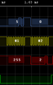
Now we’ve sent a 6 which is Write Enable and we don’t expect anything back. This command needs to be sent every time before we actually write to the EEPROM.
Query 4
Now we send 5 to read the status register, this time we receive 2. The result 2 means the Write Enable Latch bit is on (look at the table in query 2) which means the EEPROM is now ready for writing. So basically we are testing to see if our Write Enable (query 3) was actually received by the EEPROM; which it was.
I’m going to start grouping queries together so it’s easier to see, as you should have the idea of it all now.
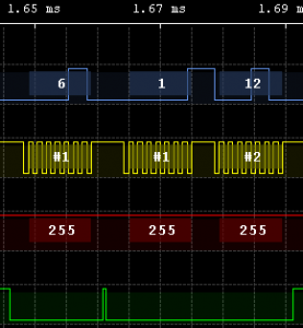
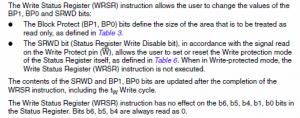
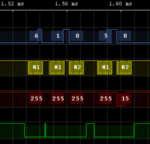
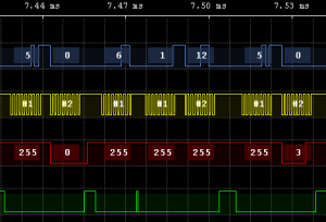
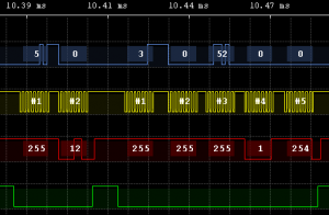
Once again we send Write Enable (6) and now send a Write Status Register (1) with the number 12 (1100 in binary). Now we’ll check the data sheet to see what Write Status Register does, page 20.
Remember in Query 2 when I said we’ll ignore some things from the Status Register, now we’ll cover 2 of those things which are the Block Protect bits, BP1 and BP0. Basically if we enable these bits, some/all of the memory will be protected from writing to, even better insurance that when we start up that nothing will write to our EEPROM!
By sending 1100, we really send 00001100 (makes it easier when looking at the table above), we enable both block bits. Note, if we were to send 1110 say as a quick way to enable the Write Enable Latch bit , the EEPROM will actually only process bit 7, bit 3 and bit 2 and ignores the rest of the bits we send.
So if BP1 and BP0 are both set (which they are) all our memory in the EEPROM is un-writeable.
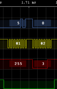
Now we’re just checking the Read Status Register (5) to see if the EEPROM is actually writing the BP bits we sent, the result received is 3 (11 binary) which it appears the EEPROM is now writing, so we better not disturb it. We can however keep checking on it to see once it’s done by continually issuing the Read Status Register (5) query.
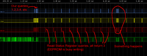
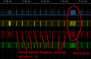
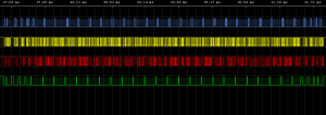
I’ve zoomed out quite a bit because guess what, they do continually issue the Read Status Register (5) query for the next few milliseconds. The result received back is always 3 and then we can see that something happens, lets see what it is.
So we have the Read Status Register and now it’s returns 12. This means that isn’t not writing any more, the Write Enable Latch Bit is off (as expected after each write) and it actually wrote our BP1 and BP0. Next they do a Write Enable (6), a Write Status Register (1) then set the bits all to 0.
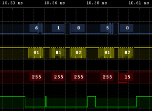
Strange, makes me think that they are just testing out the functions in the EEPROM to make sure it’s operational? Next is a Read Status Register (5) and it comes back as 15, because the BP1 and BP0 are still set and the EEPROM is now writing. Once it’s finished it will remove the BP1 and BP0.
We have the usual few milliseconds wait then we have some more data.
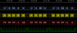
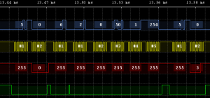
So we have the Read Status Register (5) and yep it comes back with 0, so it’s cleared BP1 and BP0; the EEPROM is now not protected from writes. We then have the usual Write Enable (6), then Write (2) which means we are going to be actually writing to the EEPROM, next comes the 16bit (2 bytes) address as 0, 69 (in hex it’s 0x00, 0x45) or more simply 0045h. The next thing that should have happened is that they should have send the byte to write but it seems like they didn’t for some reason?
They then run a Read Status Register (5) and well the EEPROM has ignored the request as it’s comes back as 2, saying only the write bit is set and that it’s not actually writing. They then read (3) the 0,0 address (0000h) and then Write Enable (6), a Write Status Register (1) then set the bits all to 0 once again, but these were never actually changed so it didn’t have to be done. Next is a Read Status Register (5) and it comes back as 3.
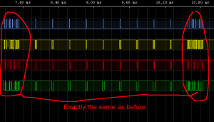
After a few milliseconds the EEPROM has finished writing and something is obviously expected to happen because they repeat the exact same bunch of queries as before 2 times, with the results being no different than before. Now after the 3 failed attempts something new happens.
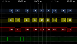
So we have the Read Status Register (5) and it comes back with 0. We then have the Write Enable (6), then Write (2), the 16bit address as 0, 0 and now actually have the data to write which is 69. So I guess that the 69 in the previous 3 attempts was supposed to be the data and not the address. Why they choose 69, who knows? Usual Read Status Register (5) and EEPROM is now writing.
Once the EEPROM finishes writing (5, 0), they then read (3) the address 0, 0 and 0, 1 then 69, 255 is received back from the EEPROM so the write they did before worked ok. After that they do a Write Enable (6), Write Status Register (1) and set it to 0 but this wasn’t needed as the status register hasn’t been changed since. EEPROM is once again writing these changes.
Now they write the value 155 to the address 0,0 and check for completion. Maybe writing the value 69 to address 0,0 was another one of their tests to the EEPROM?
It actually looks like they are now ready to use the EEPROM for real this time as they read address 0,0 to receive 155 back. After which they begin to read 2 bytes from the other addresses of the EEPROM such as 0/98, 0/102 and 0/116.
They then start reading 8 bytes from the address 0/124 to 1/56, so they have read 187 bytes in total (0/124 to 0/255 and 1/0 to 1/56). Maybe this is some kind of firmware?
After that they then read the addresses 0/102, 0/110, 0/118, 0/112, 0/112 again, 0/119, 0/114, 0/114 again, 0/120 and 0/116. Possibly some configuration variables?
Now what’s strange is what happens next, the CS line is high and they seem to send the same signal 16 times, this obviously isn’t going to the EEPROM but to another device, the question is to where? As far as I can see there isn’t any other device on the PCB other than the micro-controller and EEPROM.
After that strangeness, they then read 2 bytes of data from addresses 0/2 to 0/82 and then that’s the end of all communication with the EEPROM. I’ve tried to change the bytes to ASCII however there isn’t much sense that comes out of it.
Lets try to press the connect button on the keyboard and receiver to see what happens.
Download here: Logitech LX310 Connect SPI 10Mhz
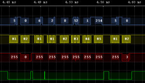
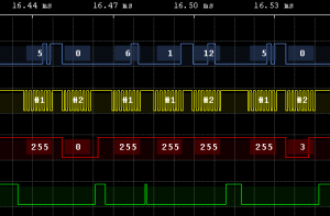
Press either the receiver connect or keyboard connect results in the same results. First we set the BP1 and BP0 to off so it stops protecting the EEPROM data, you’re probably thinking when did it get turned on because we see the result from Read Status Register (5) is 15? Well it doesn’t when starting up, it only gets turned on after you press the connect button which in my case I’ve pressed it a few times.
Now for the more interesting part, we write 2 bytes to address 0/52 which is 1 and 254. Then they turn on the BP1 and BP0 bits. In the next part they check to see that the write was successful, turning on BP1 and BP0 seems a bit of an overkill to me…
Because guess what, they turn BP1 and BP0 off again! Now we write 2 bytes with the same values as before (1 and 254) this time to address 0/50. Now why they need 2 places to store the same result, could be one for the keyboard and the other for the mouse? Next they turn on BP1 and BP0 again.
Then they check if the write was successful like before and that’s the end of the connect process. Once you press connect again, it changes the values stored to 0 and 255. Press it once more and it goes back to 1 and 254, so there are only 2 channels the wireless keyboard/mouse operates on.
And that’s a wrap for this post. I found this quite interesting myself maybe I’ll look into other gadgets to do this to :), I have one in mind which is a wireless home power meter.
