Last week we built an automatic voltage switching circuit and now it’s time to apply this circuit to the Standalone Temperature Logger (SATL).

Let’s bring up the new schematic for the SATL with the voltage switching circuit. As you can see like last week, we separate the grounds of the voltage sources – the 3V battery and USB. Notice that CRTGND is not the same as GND, CRTGND connects to the mostfet drain/schottky diode.
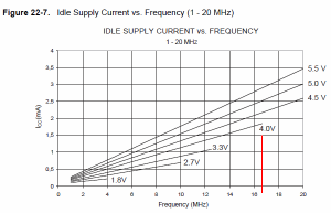
There is a downside to this circuit which is that there is a voltage drop when running from the USB side due to the diode. The USB voltage can vary between 4.75V to 5.25V and the good news is that our ATtiny85 can run fine at 16.5MHz whilst at 4.0V.

If the USB voltage was really 4.75V, we would just make it to 4.05V but we want the best possible voltage even if it was 4.75V. Instead of using just a standard diode we’ll use a schottky diode which can provide a lower voltage drop of 0.3V instead of the 0.7V from standard diodes.
Clock speed
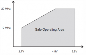
We could just wire it all up and run it but we have a problem. If we insert the battery, by default we are running at 16MHz (using the PLL clock) which is outside of the safe frequency range of 3V when powered by the battery. Before we go any further please take a look at my video called Change the ATtiny85 clock speed on the fly which will give you an idea of how we can change the clock speed using the clock prescaler.
What we’ll need to do is somehow have the ATtiny85 reduce it’s clock speed when powered on. When the ATtiny85 comes out of the factory it’s clock speed is 1MHz even though it uses the internal 8MHz oscillator. It does this by setting a fuse bit (CKDIV8) to divide the clock by 8 which gives us the 1MHz.
-U lfuse:w:0x61:m -U hfuse:w:0xdf:m -U efuse:w:0xff:m
So let’s just set this CKDIV8 fuse bit on again (we turned it off when we were playing around with V-USB and set our clock to PLL) which will make it run at 2MHz (16MHz / 8 ) when power is applied to it. After it’s powered on, we could then reduce the clock even more to give our desired clock of 1MHz and just ramp back up to 16MHz when we detect that the USB is connected.
 void setup(void) {

  // Change 2MHz to 1 MHz by changing clock prescaler to 16
  CLKPR = (1<<CLKPCE); // Prescaler enable
  CLKPR = (1<<CLKPS2); // Clock division factor 16 (0100)

  sei(); // Turn on interrupts
Now that our ATtiny85 will always default to 2MHz when power is initially connected to it we’ll go to our setup function in setup.c and change the clock speed from 2MHz to 1MHz using the method from the video I linked to before. We set the prescaler enable bit to 1 and then write the clock division factor we would like, in our case 16 to give us 1MHz (16MHz PLL / 16 division = 1MHz).
if (usbConnected) { // Send data from EEPROM to USB
  cbi(TIMSK, TOIE0); // Turn off Timer0
  PORTB |= (1<<ledPin);

  // Increase clock speed to 16MHz
  cli(); // Disable interrupts
  CLKPR = (1<<CLKPCE); // Prescaler enable
  CLKPR = 0; // Clock division factor 1 (0000)
  sei(); // Enable interrupts

  startUSB();
  transferData();

  // Decrease clock speed to 1MHz
  cli(); // Disable interrupts
  CLKPR = (1<<CLKPCE); // Prescaler enable
  CLKPR = (1<<CLKPS2); // Clock division factor 16 (0100)
  sei(); // Enable interrupts

  PORTB &= ~(1<<ledPin);
  sbi(TIMSK, TOIE0); // Turn on Timer0
}
Now over to our main function in main.c, let’s add the code to change to 16MHz when USB is detected and then change back to 1MHz after the USB transfer is complete; we need to disable interrupts before doing so and then re-enable them.
Changes to ADC, Delay and BOD
ADC
Another thing that needs to change is the A2D prescaler for the ADC.
// Set A2D prescale factor to 8
// 1 MHz / 8 = 125 KHz, inside the desired 50-200 KHz range.
sbi(ADCSRA, ADPS1);
sbi(ADCSRA, ADPS0);
// Enable A2D conversions
sbi(ADCSRA, ADEN);
Previously the A2D prescaler was set by checking the F_CPU but since the definition would be 16.5MHz it would result in a prescaler of 128 which won’t work when we are at 1MHz (as 1MHz / 128 = 0.007 KHz) so let’s set the prescaler manually ourselves at the end of the setup function. The reason we don’t touch F_CPU is because the it’s needed to be at 16.5MHz for USB code to work.
Delay
Because we changed the clock speed this means that any calculations made with F_CPU whilst we aren’t connected by USB is going to be incorrect which includes the use of delays and millis.
// Delay ms when we are at 1MHz by dividing by 16.5 as our F_CPU at compile time is 16.5MHz
void delay_ms_at_1mhz(int ms) {
  _delay_ms(ms / 16.5);
}
The easiest solution is to divide all of our delays by 16.5 in a new function called delay_ms_at_1mhz and set this to replace all _delay_ms in our code when we aren’t connected to USB.
#define clockCyclesPerMicrosecond() (F_CPU / 1000000L )
change to
#define clockCyclesPerMicrosecond() (1000000L / 1000000L )
For the millis side we can easily change the F_CPU in the definition of clockCyclesPerMicrosecond to be 1000000L (1MHz) to correct it.
Brown-out Detector
Since we use USB we are now using the ATtiny85-20PU microcontroller which has the voltage operating range of 2.7 – 5.5V, this means our BOD needs to change to something a bit higher.
-U lfuse:w:0x61:m -U hfuse:w:0xdd:m -U efuse:w:0xff:m
The BOD voltage level that we need to use now is 2.7V.
Download the updated project here: SATL_v2.0_Beta_3
Edit: I have discovered that using the BOD with a 3V coin cell isn’t always a good idea when the battery has been used a bit and is at about 2.95V. For me when connecting power to the MCU to start up, it would drop to 2.75V and be draining ~0.5mA. Use -U hfuse:w:0xdf:m to turn off the BOD which I highly recommend.
USB minus pin and Zener diode
If you checked the schematic you would have noticed that both the 3V and 5V VCC’s are connected together. This means that we can no longer just digitally read the USB minus pin to check if USB is connected because it will always result as being true. Instead we’ll have to use the ADC to check it, if we are on the 3V battery at most our ADC will read 3V but once we are on the 5V USB we’ll see something like 3.6V because of the 3.6V zener diode.

(Picture thanks to Electronics Tutorials)
Now you’d think that what I just said was correct but it turns out that zener diodes don’t work that precisely especially if you don’t flow much current through it. You need a minimum amount of current to have the zener diode be in the “Zener Breakdown Region” which is when it really becomes ~3.6V. This minimum amount of current is denoted by Iz (min) and the maximum current is Iz (max).
However some of the datasheets for zener diodes don’t contain this graph at all, for example the Fairchild 1N5227B that I’m using only has a table. In that table you can see the 3.6V as the typical Vz and 20mA as the current they were testing the diode at. From my testing, I found that when connected to 3V with the 1.5k resistor the zener’s voltage was 2.21V and the whole circuit used 0.46mA, that’s a big problem as this means when we power the circuit from the 3V battery it will always use 0.46mA! I’m glad I tested things out.
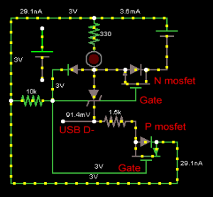
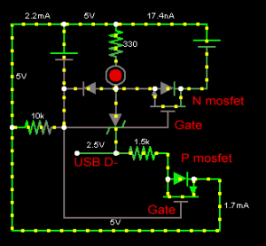
The simplest solution to this is to add another component to our automatic voltage switching circuit. We already have the N channel mosfet to turn off when 5V is detected so we can do the opposite of that by using the P channel mosfet; it’ll turn on when the 5V is detected. So once it is on it will make VCC flow to the 1.5k resistor and then to the USB D- pin. This means we can ignore our attempt to switch over to the ADC and just go back to digitally reading the pin.
Here is the circuit at 3V. Notice that the N channel mosfet is on and the P channel mosfet is off, both mosfet’s gates are connected to the same location. The voltage going to USB D- pin is 0 so if we were to read the pin it would show as off.
Now for the circuit at 5V. The N mosfet is off as expected but the P mosfet is now on because it’s gate is -5V (doesn’t show in the picture) which allows the USB D- pin to read ~2.5V. So now we read the pin it’s high, our problem is solved!
Here is our new schematic.
Battery life re-calculation
Since we are running from a 3V battery, the battery life won’t be as long as the SATL v1 which used the ATtiny85V-10PU (1.8V – 5.5V). Let’s bring up a CR2032 battery datasheet, I’m using the Energiser datasheet.
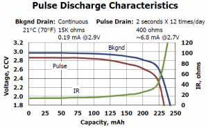
We take a look at the “Pulse Discharge Characteristic” graph in which they test the battery to see how long it lasts in two different configurations, a background constant drain or a pulsed drain. For the SATL it’s a combination of the two as it wakes us every 4 seconds from the watchdog timer but we’ll just look at the background drain (blue line). Even though I know we won’t be using a continuous drain of 0.19mA (ours might be 0.02mA) we’ll use this graph as a worst case scenario. If we compare the capacity when the voltage drops to 2V (240mAh) vs 2.7V (215mAh), we only lose about 25mAh so it’s not as bad as I thought.
Now we will test our circuit to see how much in reality it takes whilst sleeping and when it wakes us after 4 seconds due to the watchdog. I observed 0.005mA (5uA) when sleeping and up to 0.3mA when waking up every 4 seconds, I found that it was only awake for up to 30ms. The number of wake ups per hour is 3600 / 4 = 900.
Let’s punch those into a battery life calculator, the result is 2.89 years! 🙂
Now we’ll test it out switching from 3V to 5V and back. It works just fine and there appears to be no cut out when changing voltage sources. That wraps up this post, the next thing to do is design a PCB for it. I’m thinking of using SMD mosfets as I don’t want to take up too much space by using TO-92 ones.


