Following from Part 4 we tested the ATtiny85 with external SRAM via SPI which worked well however we don’t have enough pins to use SPI and V-USB on the ATtiny85. In this part, we will be upgrading to the ATtiny84.
The ATtiny84 has most features that the ATtiny85 does however I found that it didn’t have the PLL clock to generate the 16.5MHz needed for V-USB when using the internal oscillator. We do have enough pins to use a 16MHz crystal which also works with V-USB.
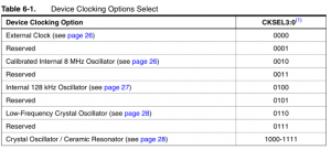
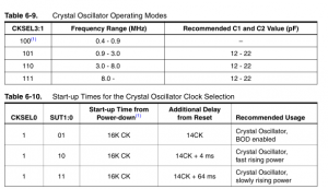
We use CKSEL as 111 for crystals higher than 8MHz. The factory default for Start-up Times is 14CK + 64ms for slowly rising power, so we’ll use that also for the crystal too.
Now we can change the V-USB usbconfig.h file to select the correct pins for the minus and plus pins, ideally you would want to use the INT0 pin.
The problems is we can only use the PB2 pin as the other PB0/1 ports are used by our oscillator and then there is reset pin. This is because V-USB doesn’t make it easy to use a PA port for the minus pin and a PB port for the plus pin.
An option provided in usbconfig.h is to modify the interrupt that’s being used so instead of using INT0 we could just use a pin change interrupt instead. I was trying to do this modification on the 2008/2012 versions of V-USB without success.
I happened to find a website of someone whom had a V-USB version 2009 working with their ATtiny84. I used that same version and their solution to the PB selection issue was to use 2 PA ports but then just connect a wire from PA0 to PB2 (INT0) so we use 2 pins as 1 pin in a sense.
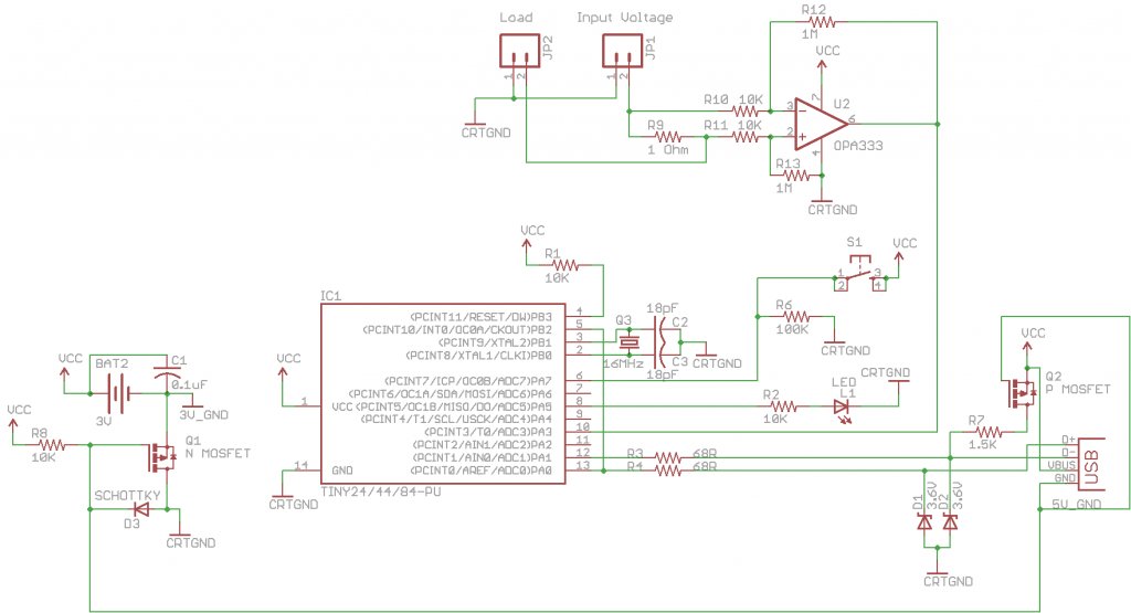
Here is our current schematic with the ATtiny84.
#define adcPin 3 // Analog input 3
#define ledPin PA5 // Output
#define buttonPin PA7 // Input
#define usbminusPin PA1 // USB D-
#define F_CPU 16000000
...
DDRA |= (1<<ledPin); // Set Outputs
DDRA &= ~(1<<usbminusPin); // Set Inputs
DDRA &= ~(1<<buttonPin);
PORTA |= ((1<<PA2) | (1<<PA4) | (1<<PA6)); // Pull-ups
...
// Pin interrupt setup
sbi(GIMSK,PCIE0); // Enable pin change interrupt
sbi(PCMSK0,PCINT7); // Apply interrupt to button pin
And the main code changes to our code shown above, mostly just changing the port pins and the pin interrupt setup.
Upon testing the circuit it seemed to work however the readings I was recording weren’t quite right because the result was fluctuating by a few mV. I decided to do an ADC reading on the ground of the circuit, the result read 7mV. I tried the ATtiny85 and it gave 2mV ADC when reading ground.
Eventually I found that if we do anything after we turn on the ADC for a reading, it can introduce noise. To test how bad the noise could be I ran the code below which is what we would be running if we did have to write the result to the external SRAM. I ran it on this circuit: 4.7V -> 1M -> ADC Input -> 10K -> GND which should give 47mV.
// Start the ADC conversion
sbi(ADCSRA, ADSC);

//Start the ADC conversion and write the previous ADC result to memory
adcMemory[adcCount] = adcResult;
adcCount++;

spi_transfer(0x02);
spi_transfer(0);
spi_transfer(0);
spi_transfer(123);
spi_transfer(213);

// Wait to be woken up by the ADC interrupt
set_sleep_mode(SLEEP_MODE_ADC); // Set sleep mode ADC
sleep_mode(); // System sleeps here
The results were pretty bad:
44
52
175
175
176
175
175
175
177
...
This means we can’t proceed with our original plan to store the result to the SRAM whilst the ADC is running. We can only sleep when the ADC is running and store the result after-woods meaning that we will have to wait about 145us for the ADC to complete and then 85us to transfer the data to the SRAM, so lets round it up to 250us. Another option is just to use an chip dedicated to ADC – maybe in one of the future versions.
Whilst looking up the ADC information I found out the we don’t have to start the ADC conversion (ADSC) because when we go to ADC sleep, it actually does it for us.
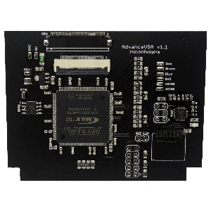
Here is the current of the Current Logger v0.3. While this isn’t what I expected to have completed in this part, we should now be able to connect up the SRAM in Part 6 (or lets hope so!).
