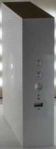
Today we’ll be taking a look at the Telstra F@st 5355 Wifi Router which supports ADSL2+/VDSL2+ on the DSL port, Gigabit WAN port, PSTN and Phone port, 2x 100Mbit LAN ports, 2x USB 2.0 ports, 802.11ac/802.11n Wifi and DECT.
I was trying to look for some screws but couldn’t find any at first until I eventually found there were 3 under the label.
The shell comes out and then you can slide the top off the case.
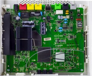
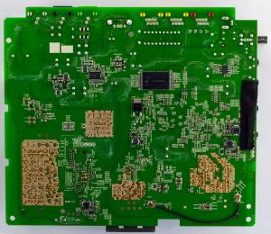
There’s a lot going on, we have a interesting large looking heatsink with a smaller ceramic one, a couple of RF cans, lots of antennas, two large 3300uF capacitors glued down and even more interesting, the back of the board with the exposed pads with it’s via’s looks pretty neat. PCB date code is 45th week of 2016.
For the power side of things, there isn’t too much going on apart from a P mosfet FDS9435A. There’s 7x DC-DCs around, most of them are MP1470s and there is an 2SB772 PNP transistor too.
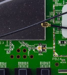
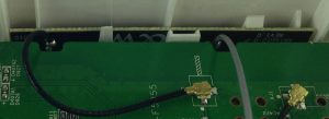
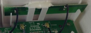
One thing you’ll notice is that one of the u.FL antenna connectors on the top board are disconnected, this actually happens when you slide the top case off but don’t lift it up properly. But it’s kind of strange that they are running a u.FL antenna only like 10cms, twice actually, one on the top board and one on the bottom board.
We have 2 external board antennas (with 2 u.FL connections each), a metal antenna and another 2 PCB antennas on the board itself, so all in all, there are 7 antennas.
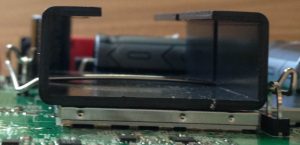
The large heatsink is just stuck on to the RF can.
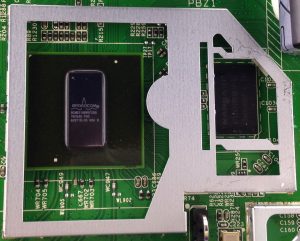
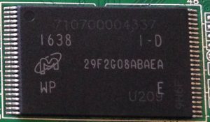
There were blue heatpads on both chips. We have the main chip, the Broadcom BCM63168 SoC which features ADSL2+/VDSL2, 802.11n, DECT, VoIP and Ethernet switching with QoS powered from a 400MHz dual-core MIPS CPU. Next to it we have the memory, a Nanya NT5CC128M16IP 2Gbit DDR3 memory and underneath we have the Micron 29F2G16ABAEA 2Gbit NAND flash memory.
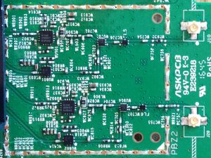
There are 4 RF lines going from the main chip directly to 2x 2 chips, one of which is a Skyworks SiGe2565T 2.4GHz power amplifier and the other chip is labelled 74 ZFJB which might doing the receiver side of things. Both chips join up to a Skyworks SKY3348 0.5-6.0GHz SPDT 50 ohm terminated switch.
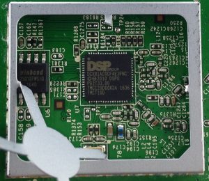
In the next RF can, we have a DSP Group DCX81 SoC that handles the DECT side of things with it’s built in digital baseband controller, analog front end, RF transceiver and power amplifier. It’s running with on an 208 MHz ARM926EJ-S and uses serial flash memory which is what the chip right next to it is, a Winbond W25Q16FW 16Mbit flash memory. The DECT RF lines are going through the two u.FL extension leads to a PCB antenna and the metal antenna.
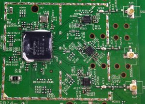
Underneath the ceramic heatsink we have the Broadcom BCM43602 chip which handles the 802.11ac 3×3 Wifi. You can see the 3 RF lines going to the 3 chips which is a Skyworks SKY85712 5GHz WLAN front-end module and then going off to the 3 u.FL connectors.
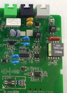
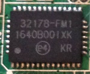
We have the usual bits and pieces for the modem/phone ports, MOVs, transformers, etc. There’s a Silicon Labs Si32919 chip and also a Silicon Labs Si32178 (on the bottom) both of which are foreign exchange station (FXS) phone solutions. We also have the ADSL2+/VDSL2+ front end chip the Broadcom BCM6303.
And that’s all.
