I’ve built a 32KB Gameboy cartridge before to add support for certain flash chips to GBxCart RW but those were wired straight through without the need of an MBC so I thought it might be interesting to jump back into CPLDs by building an 2MB Gameboy cart.
We have a few options when building a Gameboy cart, use 5V Flash chips (which are pretty rare these days) with 5V SRAM chips or go 3.3V Flash/SRAM chips and use level shift transceiver with direction control to interface with the Gameboy’s 5V logic. Because this is my first real cart, I’m going with easier the 5V flash/SRAM chip option for the moment.
(sneak peak of the cart running a game)
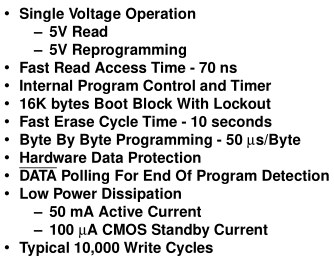
The only flash chip I have on hand is the 512KB AT49F040 so I’ll use that at the start and then we’ll transition to the 2MB AM29F016B in a later part once it arrives. For the MBC, I have an Altera EPM3032 CPLD handy so we’ll go with that, it runs off 3.3V so we’ll need an LDO for it and the inputs accept 5V logic.
Initial Planning
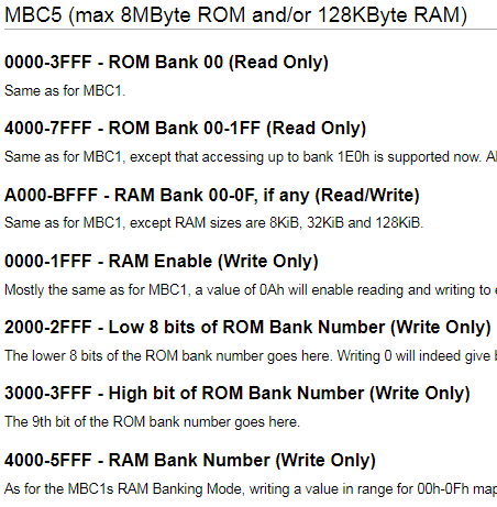
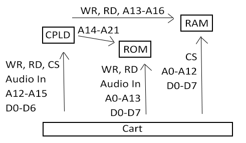
Let’s get started, firstly we’ll review the MBC5 documentation to determine which addresses the CPLD will need to read for changing ROM banks/RAM banks, etc. The lowest address is 0x0000 – 0x1FFF for RAM enable, the highest bit of that address that’s a 1 is A12 so that’s where we will start. The highest address is 0xBFFF when accessing the RAM, so A15 is where we will end, that makes 4 bits which are needed for listening to incoming MBC requests.
We also need to read the data bits however because we are only building a 2MB cart, we don’t need to support the full 512 banks of MBC5, just 128 banks (128 x 16KB = 2MB) is needed so we can just read bits D0 to D6, the low 7 bits of the ROM bank number.
Other pins we’ll need is WR, RD, CE pins because we’ll need to know if we are writing/reading to the ROM or RAM which is done by WR or RD going low along CE going low or if we are performing MBC requests for which WR goes low while the rest stay high. I’ve decided that I will be using the Audio In pin to go to the Flash’s WE pin, if this pin is low then we are writing to the flash (you’ll see why we used this pin instead of WR) so we’ll monitor this pin as well.
The way that MBC requests are configured makes everything easy to work with, the ROM (0x0000 – 0x7FFF) is separated from the RAM (0xA000 – 0xBFFF) by the address space so there is basically no way you could accidentally read the ROM if you wanted to read the RAM. Since 0x7FFF is the end of the ROM read, you can tie the ROM CE pin to A15 (0x8000) which is what I’ve seen before.
When A15 is high (0x8000 or above), you aren’t reading the ROM anymore, so we can also feed WR and RD directly to the ROM and it will ignore those lines for addresses higher than 0x8000. But in my case I can’t do this (due to the 512KB flash chip’s write cycles, more on this later), so I will tie the flash’s CE pin to ground for the moment. For the RAM, the WR, RD pins will need to be handled by the CPLD while we can pass through the CS pin because nothing will happen unless the RD or WR from the CPLD goes low.
How the Gameboy accesses the ROM/ROM
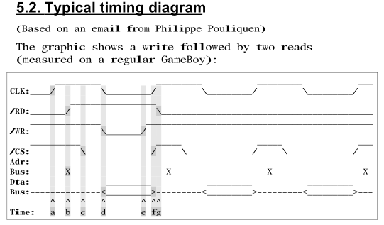
It’s a good idea to understand how the CPLD will fit in with how the Gameboy accesses the ROM/RAM. I happened to stumble upon a timing diagram from the Gameboy manual, they also include a brief description of what’s going on. With CPLDs it’s highly recommended that logic should always be clock based, so the state only changes when the clock goes high or low.
The problem with the diagram is it shows that a lot of things happen when the clock signal is high and low and also in-between, the CPLD I chose can only trigger off one side of the clock edge so that’s a problem. We could try and combine multiple signals such as RD, WR and CS into an AND/XOR gate and make a clock signal out of that but it still doesn’t give us what we need.
(Queue dramatic music)

So it looks like I’m going to be having the CPLD all latch based, checking on RD, WR, CS and Audio In. I’ll be simulating the design in ModelSim to test everything works as intended before giving it a go in the real world.
ROM configuration
As we know when the Gameboy reads 0x0000 to 0x3FFF, the ROM bank will always be bank 0, this allows us to wire A0 to A13 directly to the ROM.
The next 16KB, 0x4000 to 0x7FFF is bank switchable which means it will need to be controlled by the CPLD, so A14 and A15 from the Gameboy will be inputs going to CPLD. Our 512KB flash chip has addresses that go up to A18, so the CPLD will have outputs acting as A14 to A18 to the flash chip.
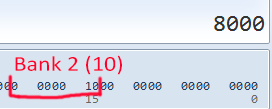
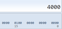
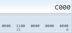
If the Gameboy switches to bank 2 and tries to read any data from 0x4000 to 0x7FFF, the CPLD itself has control of A14 to A20 (for 2MB), so for bank 2, it will set A15 high. The end result is that the Gameboy will really be reading from 0x8000 to 0xBFFF. If we didn’t have control of the A14 pin and weren’t ignoring it, it would be selecting bank 3 instead and would read 0xC000 to 0xFFFF.
RAM configuration
Because we’re still planning things, let’s briefly look at the RAM side of things too. The Gameboy reads it at 0xA000 to 0xBFFF (8KB / 0x1FFF), the two high bits that are set for 0xA or 0xB are A15 and A13. We will need to have control of the address lines A13 and higher so that only 0x0000 to 0x1FFF would pass through to the RAM directly (A0 to A12) and the rest is controlled by the CPLD.
The maximum memory supported for MBC5 is 128KByte, the highest bit would be A16 so the CPLD would need to control A13 to A16.
Here’s a quick diagram of how it looks like at the moment (we could also just have the RAM’s CS controlled by the CPLD and let WR/RD go direct from the Gameboy to the RAM).
Variables
// Inputs
input [3:0] inputAddress; // a12 - a15
input [6:0] inputData; // d0 - d6
input inputCE;
input inputRD;
input inputWR;
input audioIn;

// Outputs / Registers
output [7:0] highAddress; // a13 - a20
reg [7:0] highAddress;

reg [6:0] romBank; // a14 - a20
reg [3:0] ramBank; // a13 - a16
reg romBankSwitched;
We will need to have a variable which keeps track of which ROM bank we are switched to, it will be 7 bits long (for 2MB) and because the default bank for 0x4000 to 0x7FFF is bank 1, we also need a variable to keep track if we have switched banks. We also need a RAM bank variable which will be 4 bits long while we are at it.
We can use a single 8 bit register/output for both the ROM and RAM as they share address lines A14 to A16, A13 goes direct to the RAM and A17 and higher goes direct to the ROM.
always @ (reset or inputCE or inputRD or inputWR or audioIn) begin
	if (!reset) begin
		romBankSwitched <= 1'b0;
		highAddress <= 8'b0;
		romBank <= 7'b0;
		ramBank <= 4'b0;
  	end
  	else begin
The first step is we use the always@ to monitor any changes on the reset, CE, RD, WR and audioIn lines. If reset is low, we reset our variables to 0.
Reading ROM
if (inputAddress <= 4'd7 && !inputRD) begin
	if (inputAddress <= 4'd3) begin // 0x0000-3FFF, Bank 0 always
		highAddress <= 8'b0; // All set to 0
	end
Once reset goes high, we begin the rest of our code. When the input address is less than or equal to 0x7FFF (or 7 as we only read the high 4 bits of the address line) and the RD pin is low, we then check if the input address is less than or equal to 0x3FFF (or 3), if so then we set the variable highAddress (A14 to A20) all low so the Gameboy can read 0x0000 to 0x3FFF.
else begin
	if (romBankSwitched) begin // Set ROM bank if it was switched
		highAddress <= romBank << 1; // Start at a14 for ROM
	end
	else begin // Default ROM bank 1 if we haven't switched ROM banks
		highAddress <= 8'd2; // a14 to 1
	end
end
Next we handle the 0x4000 to 0x7FFF addresses. If the rom bank has been changed, the romBankSwitched variable is true, then we transfer over the rom bank that was selected and left shift it by 1 so that it starts at A14 instead of A13 (because A13 goes to the RAM). If the rom bank hasn’t been switched as yet, we set the default bank to 1.
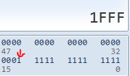
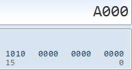
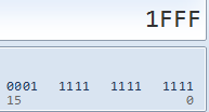
Here’s how rom bank 1, 2 and 3 would look like to the ROM, then the Gameboy would just change A0 to A13 to suit what it wanted from those banks. Remember that we don’t pass through A14 from the Gameboy to the ROM, it’s all controlled by the CPLD.
Switching ROM banks
// 0x2000-2FFF - Low 7 bits of ROM Bank Number (Write Only)
if (inputAddress == 4'd2 && !inputWR && inputRD && inputCE && audioIn) begin
	romBankSwitched <= 1'b1;
	romBank <= inputData;
end
For switching rom banks, we just check if the input address is 0x2xxx (we only check for the 2), if WR is low and if all the other lines are high. If so, then we set the rom bank switched variable, read the input data and store it to our rom bank variable, easy.
Writing to the Flash
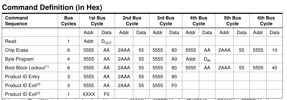
As I’m using the 512KB AT49F040 flash chip for the moment, the program write cycle starts off with 0x5555, 2AAA where as other chips start with 0x555 or 0xAAA. The problem is that with 0x5555, the A14 pin will be 1 but since the CPLD ignores this bit as mentioned before, 0x5555 will never make it to the ROM unless we switched to bank 1, did the write cycles and then switch back to the bank we needed before doing the final write cycle; too complicated and it would slow things down.
// ROM writing (audioIn low), pass through a14-15 OR with romBank
if (!audioIn) begin
	highAddress <= ((romBank & 7'h7C) << 1) | (inputAddress[3] << 2) | (inputAddress[2] << 1);
end
The solution I went with is to check if the Audio In pin is low, just pass through A14 & A15 and OR them with the current rom bank, this way we override what the rom bank should be when we are writing and on the last write cycle the rom bank applies correctly as A14 & A15 will be low. If we went with WR instead of the Audio In pin, the write cycle of 0x2AAA would collide with the rom bank switching (0x2000 – 0x2FFF) so it would switch banks by mistake.
When we switch to the 2MB AM29F016B, all of this won’t be needed as the flash write cycle is 0x555, 0x2AA, etc and it doesn’t touch A14, so then we will be able to use WR instead of the Audio In pin. (Edit: Actually the 4th write cycle might be affected but it wouldn’t matter as it would always be bank 0 when writing to 0x2000-2FFF)
uint16_t bank = 0;
while (bank < romBanks) {
	currAddr = 0x0000;

	// Set start address
	set_number(currAddr, SET_START_ADDRESS);

	// Read data
	while (currAddr < endAddr) {
		if (currAddr % 0x4000 == 0) { // Switch banks here just before the next bank, not any time sooner
			set_bank(0x2100, bank);
			bank++;
		}

		com_write_bytes_from_file(GB_FLASH_WRITE_64BYTE, romFile, 64);
		com_wait_for_ack();
		currAddr += 64;
		readBytes += 64;
		...
As we are passing through A14 & A15, we can’t use the regular method to write to the ROM because when reading bank 1, 2, etc, A14 will always be 1 since it’s being passed through. So instead of just staying in 0x4000 to 0x7FFF and switching banks, I’m using the whole address space 0x0000 to 0xFFFF. Once again this all won’t be needed once I receive the other flash chip, this is mostly to get things up and running as is.
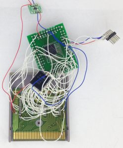
Here’s how it all looks at the moment.
After finding a game that was 512KB in size, MBC5 which didn’t have any SRAM, I wrote the flash and read it back successfully, it was time to test the game out on a real Gameboy. As you saw on the video at the start, it works!
Once the 2MB flash chip is received, I’ll swap it out, test out a 2MB ROM, add in the SRAM memory and it should be good to go – check out the next part.
Parts:
Part 1: CPLD as the MBC and adding Flash as our ROM
Part 2: Adding the SRAM
Part 3: PCBs arrived, Adding some MBC1 support and troubleshooting a few games
Part 4: Adding Multi-game support
Part 5: Using 32KB FRAM and Adding MBC1 2MB ROM Support


Hey Alex, great project. I’ve made a GB cart in the past too (details here: https://tinkerer.us/projects/homebrew-gameboy-cartridge ) and have long wanted to make a version like this. If you run into any issues, or need help testing something, contact me on twitter @Dillon1337. You could refer to this design: https://www.tindie.com/products/JRodrigo/flash-cartridge–2mb–4mb–for-gameboy/#specs schematics are available, but I haven’t found the code for the CPLD. He also often sells out, so you could sell the cartridge because there seems to be a demand for it.