Following from Part 5 we moved to the ATtiny84 so we could have more pins in order to use SPI and V-USB together and we found that we really shouldn’t be doing anything whilst the ADC is running. In this part we will be upgrading to the ATtiny44A, connecting the SRAM and updating our schematic.
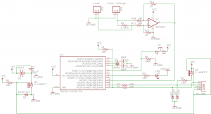
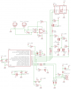
Above is the schematic from the last part.
Change to ATtiny44A and voltage switching circuit
Now it’s time to add in the SRAM however we need to find a way to keep it running at between 2.7-3.6V which means that the current voltage switching circuit we used before won’t work.
The easiest way is to use 2 diodes – one going from 3V to the 5V USB which will allow the ATtiny to be powered by the 3V or 5V, not allow the 5V to recharge the 3V battery and allow the SRAM to always be powered when there is a 3V battery. The next diode goes from the 5V USB to ATtiny just before the other diode, so our D- line will only read as high when the USB is connected and read as high when the battery is connected (used for detecting whether the USB is connected).
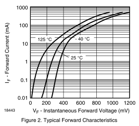
The diodes introduce a problem, our 3V battery with the schottky diode could drop to 2.7V or less if we sourced 2-3mA but the ATtiny84 20MHz model only goes from 2.7V to 5.5V.
Luckily for us the solution is to use an ATtiny44A which supports up to 20MHz and whose voltage can range from 1.8V to 5.5V so we get the best of both worlds.
2.7V ATtiny with 3V SRAM
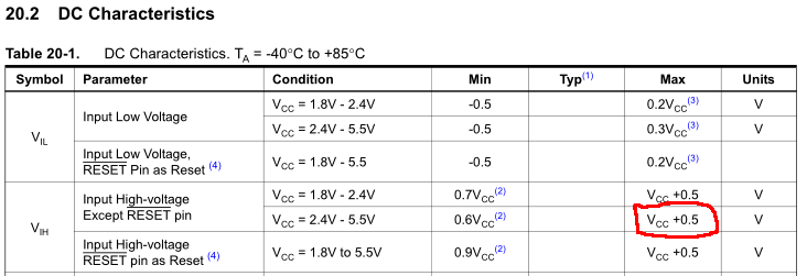
Next we need to check how much over the VCC that our ATtiny44A can support for inputs, this is because when we run from the 3V battery, our ATtiny44A might be getting 2.7V whilst our SRAM would be getting 3V.
It does look like the ATtiny44A can support VCC + 0.5V, it would allow us to go to 3.2V for an input as the maximum assuming, so we are all good in that respect.
5V ATtiny with 3V SRAM
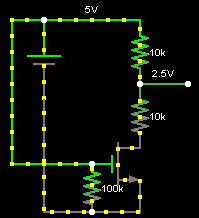
Now we need to check what will happen when the USB is connected, the ATtiny would have 4.7V and when communicating with the SRAM at 3V, the SRAM would be damaged. To solve this, we just use resistor dividers for the 3 outputs of the ATtiny’s SPI – clock select, clock and data out.
Lets assume the worst case scenario, our ATtiny44A is running at 4.7V and it’s output is a bit lower, lets say 4.3V from one of the pins (the datasheet says output would be 4.3V @ 10mA when 5V supply but we won’t ever use more than 0.1mA) so the output from the resistor divider would give 2.15V.
We check the SRAM datasheet which says input high-level voltage is 0.7 x VCC which gives 2.1V so we are barely just above the high-level voltage. But we can’t just leave the resistor divider in place because it will divide our voltage when we are operating from the battery too – would give 1.5V.
A simple N channel Mosfet connecting the resistor divider to ground is a simple solution and we can have it switch on once the USB VCC is detected.
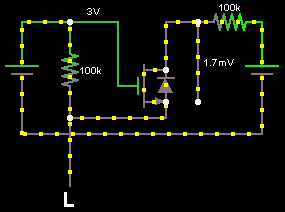
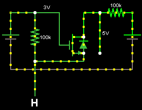
Next we do the 1 output from the SRAM to the input of the ATtiny’s SPI – the data in; we need to convert 3V to 4.7V. I found a Sparkfun Level Converter which utilities an N channel Mosfet in such a way that you can level shift a lower voltage to a higher voltage. The Bi-directional level shifter for I²C-bus and other systems datasheet by NXP on page 10 explains in detail how the circuit works.
Basically what happens is when the output is low (sink), current flows through the 100K resistor on the left which switches on the Mosfet as the Vgs is 3V, this in turn allows the 5V on the right side to flow through the 100K resistor on the right and gives us a reading of 0V (1.7mv).
Once our output goes high (source), no current flows through the resistor on the left so the gate and source are both at 3V so the Vgs is 0V thus the Mosfet is off. No current flows through the resistor on the right so we have a high on the right hand side as 5V. Technically instead of our resistor divider and Mosfet we could use this circuit as it uses the exactly the same parts, the only downside is that when the output is low it will continually drain 30uA.
Testing
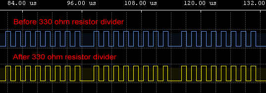
At 3 volts, my SPI test blinking program worked fine. Upon testing the 5V USB I found that sometimes it wouldn’t blink at all and had to re-connect it a few times to make it work. I measured the 10K resistor divider and it gave the correct voltage expected. I decided to use my logic analyser to measure if there was a propagation delay between the signal coming into the resistor divider and signal coming out.
With a 10K resistor divider there certainly is a propagation delay.
I decide to use some 330 ohm resistors instead that I had lying around, there doesn’t appear to be any propagation delay and it worked fine this time.
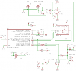
Above is our new schematic. Now all that’s left to do is to do the testing when connecting the op-amp and finalising the code.





Thanks for posting these, lovely work!