Ever since I built my 4 bay 3.5″ NAS using the Raspberry Pi which was placed inside a Netgear NV NAS enclosure, I’ve been wanting to make a single bay NAS with a 2.5″ drive to use as a small file server or for backups. I’ve decided that I’ll use it for remote backups in which I’ll use rsync over SSH from my linux server to backup some of my data at night.
(sneak peak)
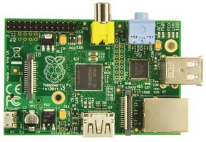
Due to my use case, I’ll need to have it operating 24×7 and don’t really have a need for an LCD or even power button, so it will be a minimalistic design. The Raspberry Pi was purchased from Element14 / Newark and this time it has mounting holes which will make things more easier for us. In terms for the power supply, I’m able to re-use an existing 5V 2A supply but otherwise I could have used my SMPS.
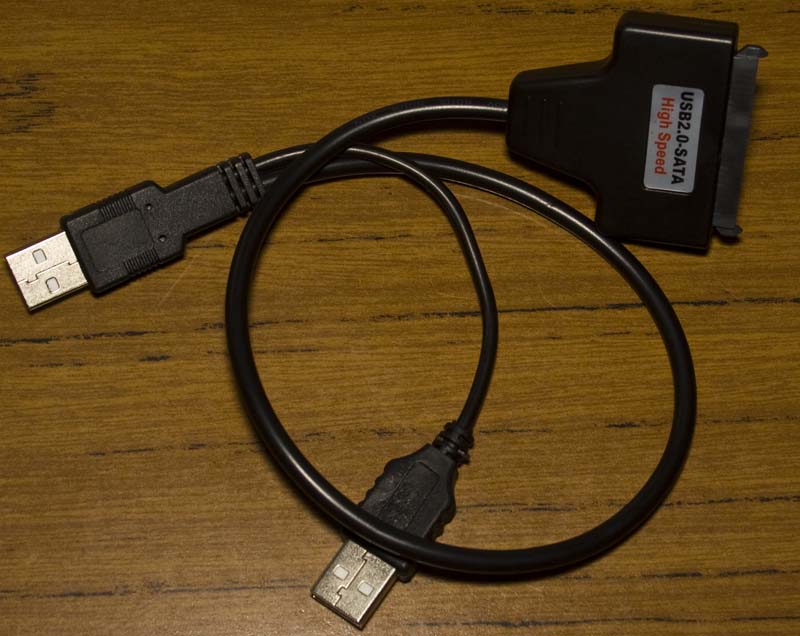
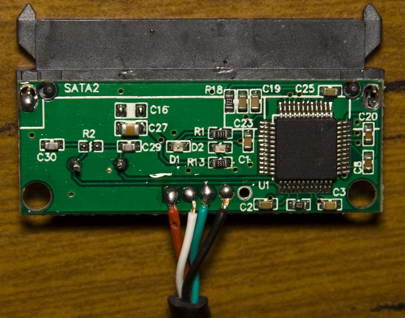
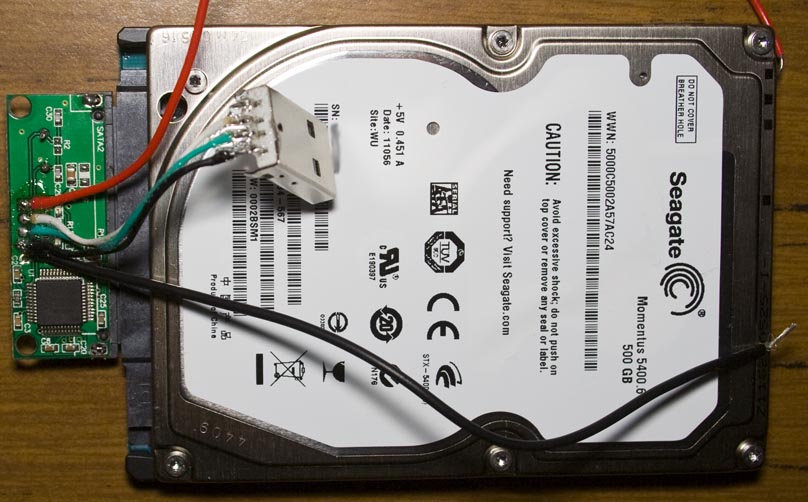
The SATA to USB adapter that I bought from Ebay was larger than I wanted so it’s time to make it smaller.
I went ahead, opened it up, shortened the USB cables, separated the power cable out (as I don’t want the Pi itself to power it), re-soldered the wires to a USB connector I had – it’s now more compact. As a side effect, this SATA adapter has quite a bright blue LED which illuminates through the acrylic case which gives it some colour. Just using a spare 500GB hard drive whilst testing.
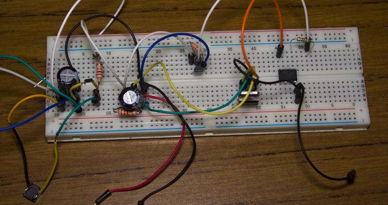
From our last post we looked at adding a transistor to the MC34063 and eventually changed to a P mosfet although we had to use a pretty large heatsink to dissipate all the heat. I decided to revist this SMPS to see if we could improve it to generate less heat, as I might have a few projects that could possibly use 5V output and 12V+ input.
I decided to build the circuit with a NPN transistor – the TIP31 however with a small heatsink with 5V @ 0.37A, it rose up to 55C so I went back to a P mosfet. I began changing all the other parts – using different diodes, inductors, resistors however the P mosfet still got pretty hot even with a small heatsink.
Thinking that the MC34063 could be causing the issues itself, I went ahead and used an ATtiny to replicate what a little bit of SMPS would be doing – pulsing an output high and low for a specific duty cycle until I reached 5V. The heat was about the same as the MC34063 but just a little less as I didn’t compensate for the load reducing the voltage.
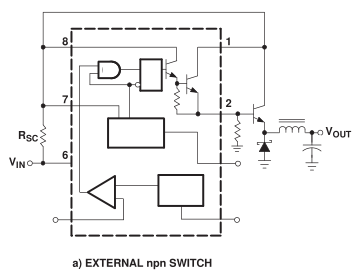
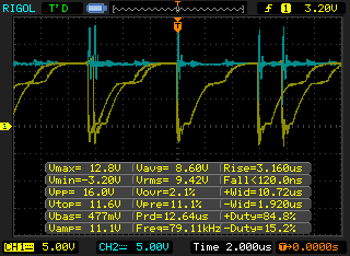
So it’s back to the IRF9540 P mosfet, after researching into it, it seems like the turn off time / capacitance is pretty important for our application, this mosfet has 1400pF input / 590pF output capacitance, 73ns rise time, 34ns turn off and 57ns fall time. On paper this mosfet seems good however as above we can see the turn off time is really 4us (yellow line, going low to high). Also there is an spike (blue) which I was able to soften down later a bit by adding a 470uF capacitor to the input VCC/GND (before I had 100uF).
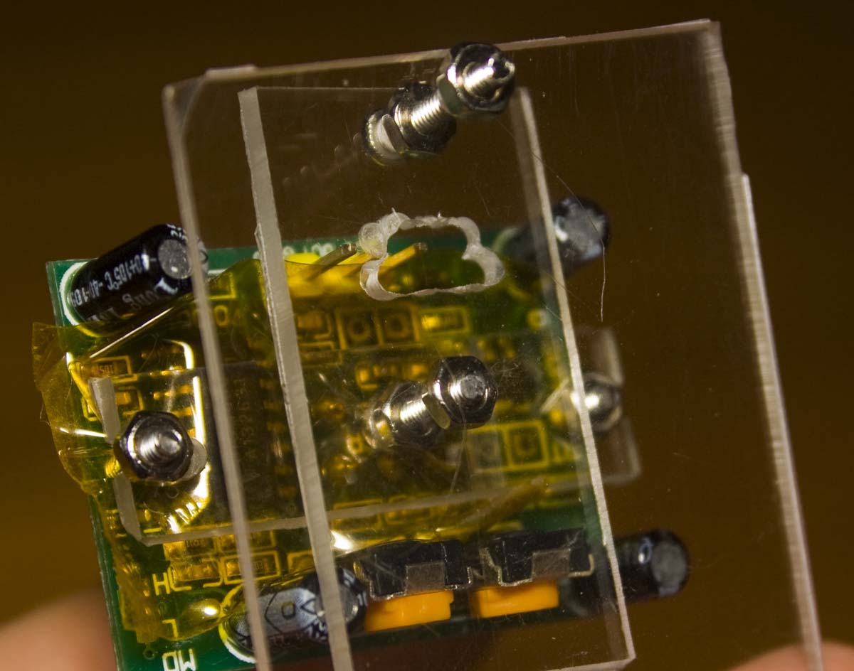
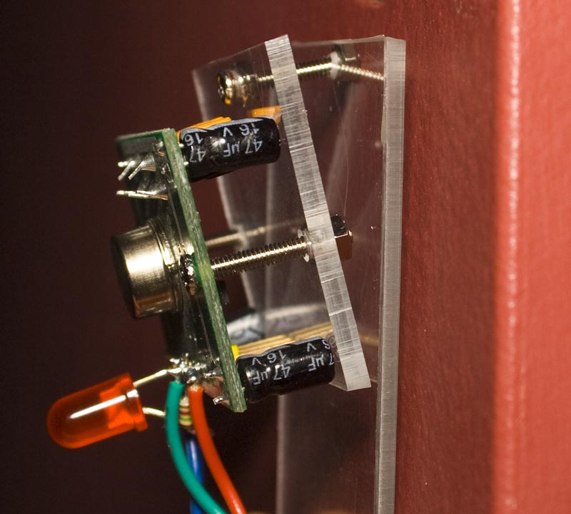
From our previous post, we made our prototyped PCBs which all worked together well. This time we just have a quick update – we’re making a few changes along with building acrylic cases/mounts for some of our boards.
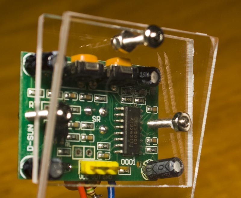
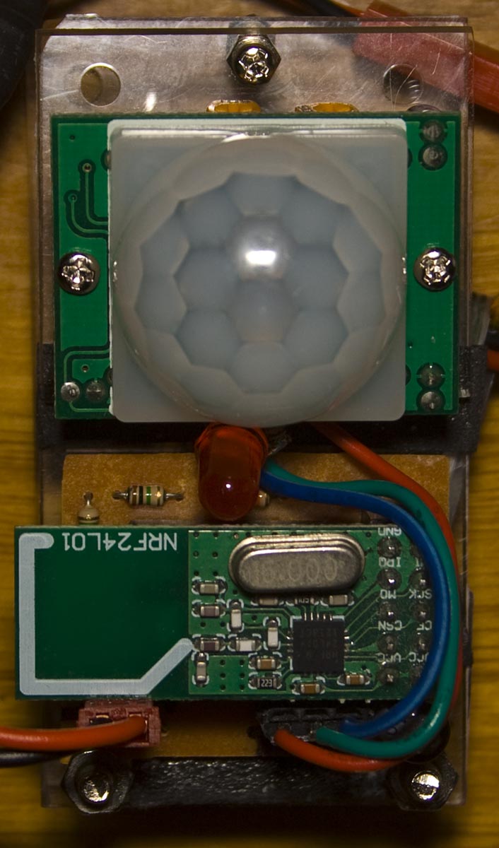
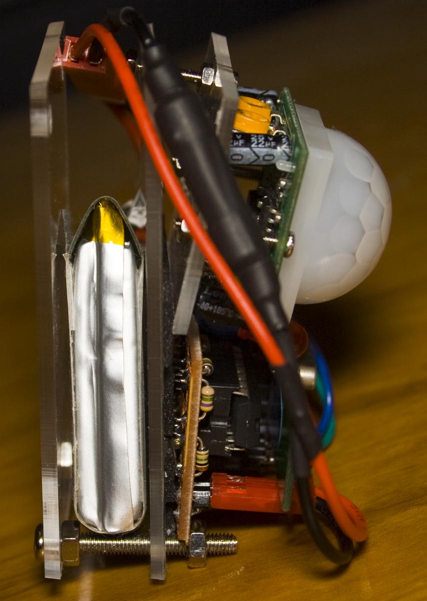
I’ve been rethinking my idea about using the existing plastic casing for the PIR, since I intended this to be a standalone alarm system I should really make my own case. We’ll need a way to mount the PIR sensor at an angle to the wall to point a bit downwards otherwise it’ll just point straight on and may not cover the whole room. Initially I started with the design above, there’s quite a bit of acrylic boards all screwed together with M2 screws.
I went for a re-design and now it’s looking better with less parts being used. I’ll need to add some mounts to the ATtiny84 PIR PCB, switch the M3 screws that hold the Lipo in place with longer M2 screws and then add a small hole at the top so I can nail the bottom board to the wall and that will sort out the PIRs.
From our last part we made some prototype boards including the buffer board and fixed the reading issues. In this part we’ll look at the software side to display the data we extract, add trigger options/sample rates, some hardware changes and possible design changes which could give us an 100MHz logic analyser.
Software for displaying our data
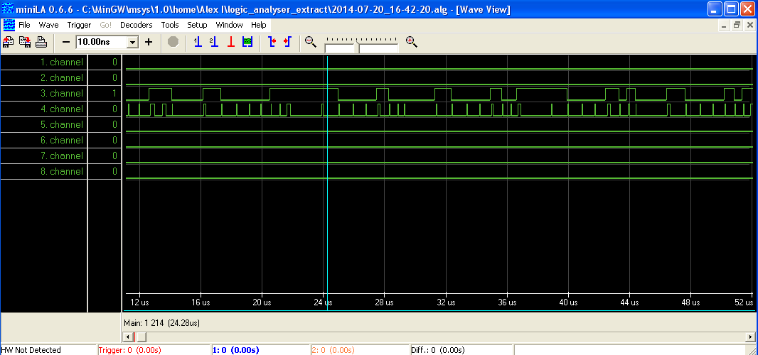
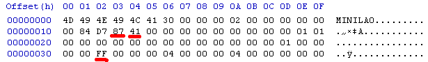
I had a look around at some software options that would just work out of the box and settled with one called MiniLA, they also had made an 100MHz logic analyser – it’s a beefier version of what I’m trying to achieve, their one has 32 channels and the CPLD/SRAM alone would cost $25-35 (about $40-50 in Australia) where as I’d like to make a small 8 channel one with USB (and it’s a learning experience for me too).
After looking around at the file format, it’s similar to how I was sending my data, so I was able to figure out how the data was formed – 00 00 FF 00 would set channel 1 to 8 all high for one time period. From the picture above, to change the time scale units from us to ns, you can change 41 to 42 and to change the time scale total length from say 2.52 to 2.62 ms you’d change 87 to 88. This should give us the flexibility to change time scale units depending on the clock we select.
Trigger/sample options
As the ATmega will act as the trigger source, I’ve been able to add options such as choosing which pin to trigger on, trigger level – high or low, trigger delay, trigger count – how many triggers we should wait for, sample rate and number of samples.
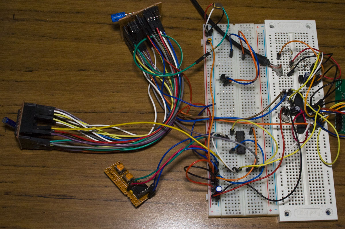
From our last part we were able to read the data from the SRAM using an ATmega but found that we couldn’t run the SRAM with a 100MHz clock and when reading the data out it was noisy/inaccurate – even re-reading the same address ranges would give different results. In this part, I’ve made some prototype boards and we’ll look into fixing the reading issues.
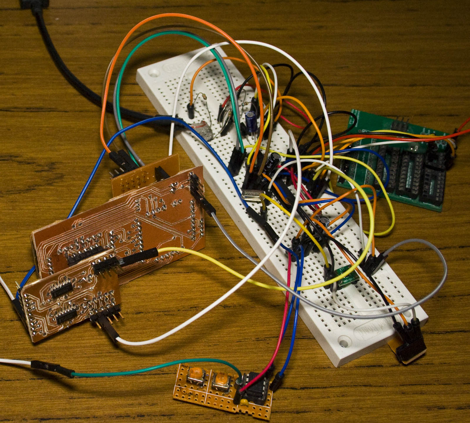
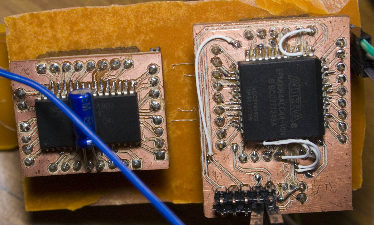
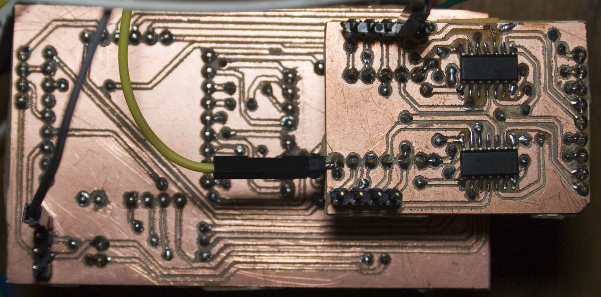
I decided to make a new board for the CPLD so I could mount it and the SRAM to a main board and also made a buffer logic board to be mounted under the main board plus there is also a very small board for the 50MHz oscillator.
For the buffer board, I’m using 2x 74LVC125 each one does 4 inputs. What I didn’t realise is that these are active low so I’ve modified my CPLD code to suit: CPLD_LogicAnalyser_v0.2
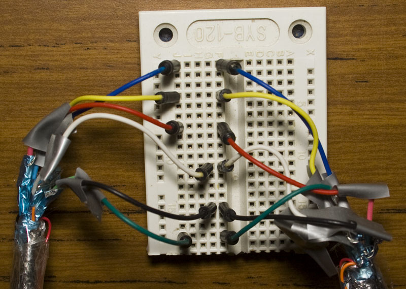
From our last part we chose the switches to use, the cabling idea to use network cables to connect to USB cables, the 7402 NOR gate to switch between inputs and gave it a test run on the VGA which worked. In this part we’ll put it all together and think about how we can add more input ports to do a 4, 8, 16 port KVM.
(sneak peak of KVM)
The first thing I did was test the 7402 NOR gate to see if there is an oscillation at startup, after a few attempts I found no issues but that you should tie unused gates to ground; even if it started in an unknown state, the state doesn’t change so it’s not too much of a concern for me.
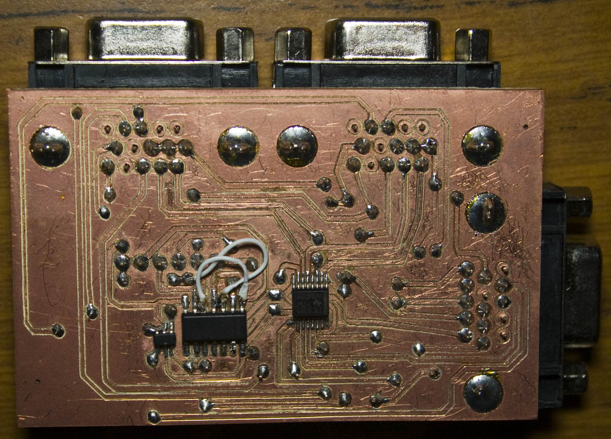
I decided to have the VGA and USB boards separate as it would be easier to route them. The VGA board was built, there was a small mistake with choosing the wrong 7402 part in Eagle so I had to make a few modifications and it tested ok, there is a 6 pin header near the center to connect to the USB board.
Ever since I built a Raspberry Pi 4-bay NAS in an existing Netgear NAS case I’ve been wanting to make a smaller custom acrylic version with just a 2.5” 750GB hard drive for either backups (like a small Synology) or a fileserver overall it should end up being quite small.
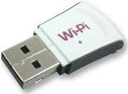
The main components of this project will be the Rapsberry Pi and Wi-pi adapter which I bought it from Element14 / Newark. Using the the Wi-Pi adapter I could make it all wireless.
Like my last NAS, I’ll be adding in a 16×2 LCD display to show the status, as I’ll be using a 2.5” drive all I’d need is a 5V 2-3A power adapter and a USB to SATA adapter of which I’ve found a better adapter that should be easier to plug the drive easier.
From our last part we switched tested the Cypress 1Mbit SRAM and read the data out with an Olimex STM32 board. In this part we’ll move to an ATmega to read out the data and use it for triggering the CPLD which will be continually sampling the inputs – the reason is because the ATmega runs slower than the CPLD so a few clock cycles will occur from when it detects the trigger to when it signals the CPLD.
CPLD Side
On the CPLD we can remove the data pins which were being used to test the SRAM and we can link WE and OE pins directly to the SRAM. We’ll re-use the writing pin to tell the CPLD to start capturing data or to be in the read mode, another pin for when we want it to trigger and it records the address minus 50 so that we can see some data before the trigger event.
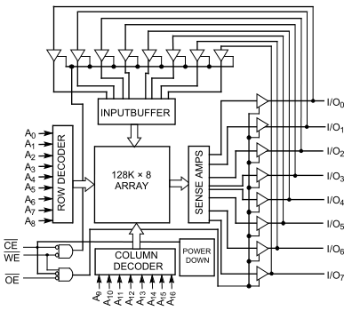
From our last part we switched to the EPM3064 CPLD for our logic analyser. In this part we’ll use the Cypress 1Mbit SRAM to store the data that we capture.
It’s a parallel SRAM which can run at 100MHz which allows us to save time compared to a regular 8 pin SRAM as we don’t have to clock in the address and clock in the data. All we have to do now is set the address pins, feed in the data and set the CE/WE pins low, the perfect job for a CPLD.
Writing and reading to the SRAM is fairly easy – to write we pull CE and WE low and to read we pull CE and WE low. In all other states the outputs are in high impendance, this allows us the option of adding more SRAM chips.
In order to test out the SRAM and the clock feed to the CPLD, I’ll have the CPLD increment an 8bit number which will be written to the SRAM and then read out with an MCU.
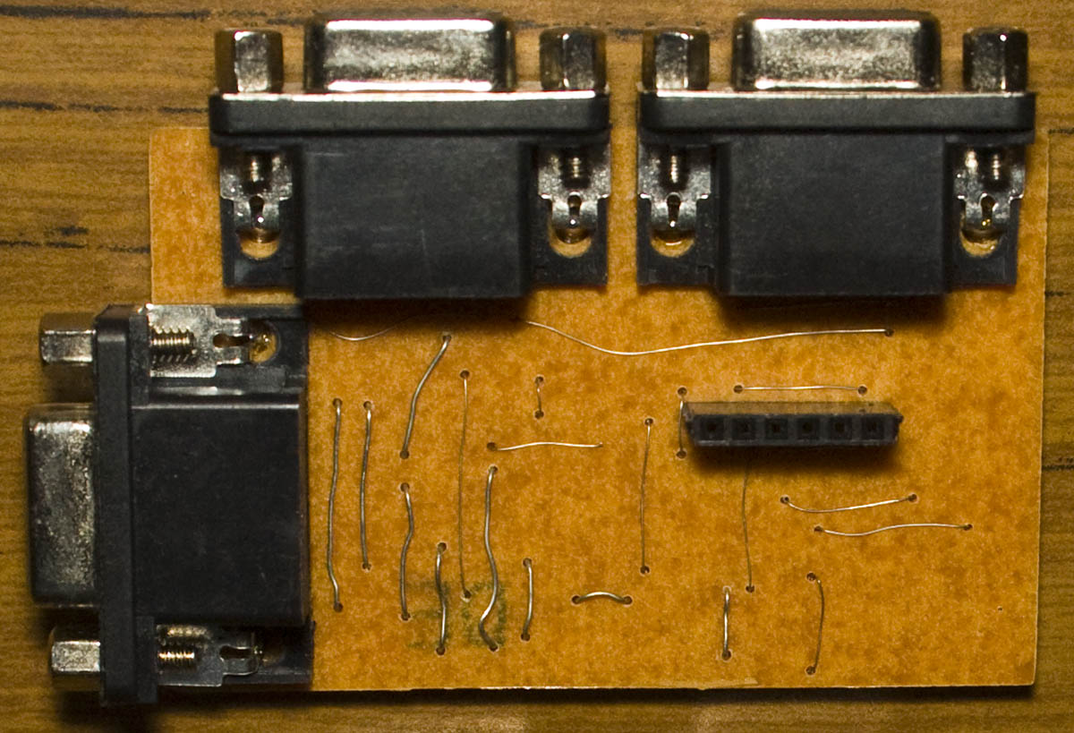
Back a few years ago when I read the EEPROM of a KVM, we did have an issue where occasionally it wouldn’t switch between computers. A KVM is a keyboard video mouse device that you switch between computers by the press of a button, they can have 2, 4, 8, 16 or more ports. Recently I did have the need for a KVM but we didn’t have one on hand, so I’ve decided it would be interesting to make my own KVM, I’ll start with a 2 port KVM first.
https://www.youtube.com/watch?v=MdbHPUWwgdk
(sneak peak of our prototype in action)
The video side of the KVM will use the VGA, firstly we need to find out how many wires of the VGA we’ll need to pass through.
After slicing some VGA cables, we just need the red, green, blue, hsync and vsync. For each wire, there is a separate ground to it – red ground, blue ground, hsync ground, etc. Firstly I tried connecting all the grounds but noticed some occasional flicker, it’s likely due to the fact that the RGB signals are analog (0.7Vpp) while the H/Vsync are digital and mixing the grounds can cause issues, you normally hear this all the time – separate analog and digital grounds when laying out a PCB. After separating them to RGB and H/Vsync grounds, it works good now.
AdvanceVGA – Play your GBA on the big screen! Swap out the LCD for our board, solder some wires, connect 5V USB and VGA and you’re ready to go.
GBxCart RW allows you to backup GB/GBC/GBA ROMs, save or restore game saves and re-write supported flash carts. Mini RW option available for GB/GBC only.
Wireless Gameboy Controller – Use your Gameboy, mGB, GBC, GBA, GBA SP, GB Micro, NDS and NDS Lite as a wireless controller on Windows, Linux, Raspberry Pi, etc, and on your NES, SNES, N64, Gamecube and Wii.